Hybrid PCB | Mixed Material PCB Built on 10 mil RO4350B + FR-4 with Depth Controlled Drill
(PCBs are custom-made products; the images and parameters shown are for reference only)
Introduction
Hello Everyone,
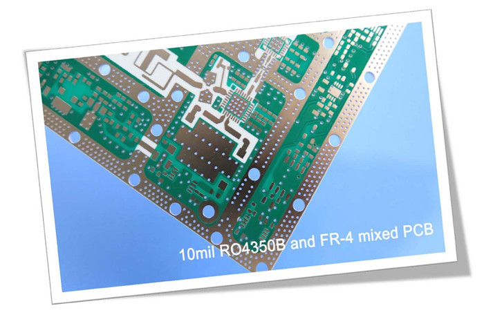
Today, we will discuss a 4-layer high-frequency PCB constructed using 10mil RO4350B combined with FR-4.
This board features a 4-layer design, which is relatively straightforward and cost-effective, making it ideal for entering new markets.
Let's Explore the Build-Up
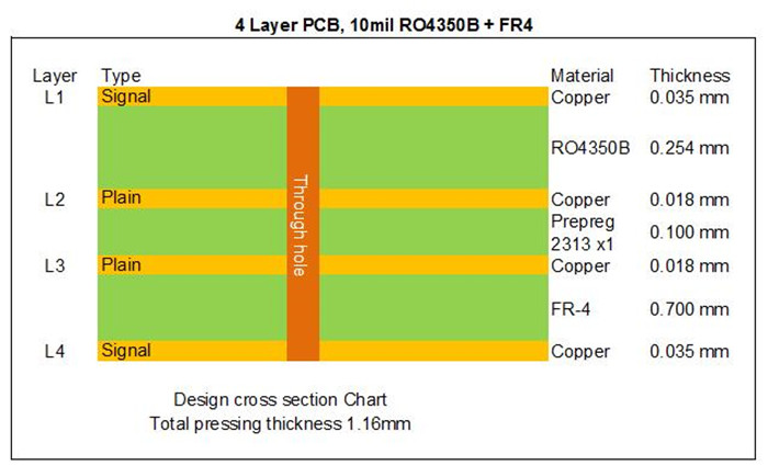
The first layer to the second layer consists of a 10mil RO4350B core material. This core has a fixed thickness, which is crucial for maintaining the electrical length of RF lines on the circuit board. The remaining layers are composed of FR-4 materials, bonded using semi-cured sheets. The inner layer has a copper weight of 0.5 ounces, while the outer layer is 1 ounce.
Cross Section Overview
The second board features a unique "depth-controlled drill" on the FR-4 side.See the build-up first.Plated through holes connect each layer, and the pads and vias are finished with immersion gold.
The second board features a unique "depth-controlled drill" on the FR-4 side.See the build-up first.
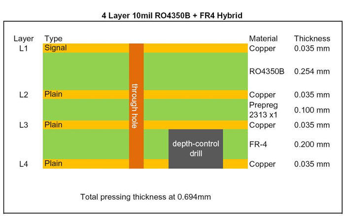
Layer 1 and layer 2 is the 10mil core. The depth-control drill is dented on FR-4 side. The whole height of this board is only 0.7mm thick.
Applications
This 10mil RO4350B hybrid PCB is suitable for a variety of applications, including:
Preamplifiers,Radar sensors,Digital transmitters,Splitter modules,GPS antennas,Communication relays,Analog transmitters,4G antennas,RF transmitters,Wi-Fi amplifiers,RFID systems,Attenuators
The Advantages of 10mil RO4350B Hybrid PCBs
1)Stable Dielectric Constant: RO4350B maintains a consistent dielectric constant across a wide frequency range, making it an excellent substrate for broadband applications.
2)Improved Signal Integrity: Enhanced performance over stack-ups made entirely of FR-4.
3)Cost Efficiency: Reduced costs compared to stack-ups using only low-loss materials.
4)Comprehensive Capabilities: Our facility meets your PCB needs from prototypes to mass production, backed by IATF 16949 (2016), ISO 14001 (2015), ISO 9001 (2015), and UL certifications to ensure quality.
Thank you for reading. Feel free to contact us for your RF PCB inquiries.
Appendix: Our PCB Capability 2022
Parameter |
Value |
Layer Counts |
1-32 |
Substrate Material |
RO4350B, RO4003C, RO4730G3, RO4360G2, RO4533, RO4534, RO4535, RO3003, RO3006, RO3010, RO3035, RO3203, RO3210; RT/Duriod 5880; RT/Duriod 5870, RT/Duriod 6002, RT/Duroid 6010, RT/duroid 6035HTC; TMM3, TMM4, TMM6, TMM10, TMM10i, TMM13i, Kappa 438; TLF-35; RF-35TC, RF-60A, RF-60TC, RF-35A2, RF-45, RF-10, TRF-45; TLX-0, TLX-6, TLX-7, TLX-8; TLX-9, TLY-3, TLY-5; PTFE F4B (DK2.2 DK2.65 DK2.85 DK2.94, DK3.0, DK3.2, DK3.38, DK3.5, DK4.0, DK4.4, DK6.15, DK10.2); AD450, AD600, AD1000, TC350; Nelco N4000, N9350, N9240; FR-4 ( High Tg S1000-2M, TU-872 SLK, TU-768, IT-180A etc.), FR-4 High CTI>600V; Polyimide, PET; Metal Core etc. |
Maximum Size |
Flying test: 900*600mm, Fixture test 460*380mm, No test 1100*600mm |
Board Outline Tolerance |
±0.0059" (0.15mm) |
PCB Thickness |
0.0157" - 0.3937" (0.40mm--10.00mm) |
Thickness Tolerance(T≥0.8mm) |
±8% |
Thickness Tolerance(t<0.8mm) |
±10% |
Insulation Layer Thickness |
0.00295" - 0.1969" (0.075mm--5.00mm) |
Minimum Track |
0.003" (0.075mm) |
Minimum Space |
0.003" (0.075mm) |
Outer Copper Thickness |
35µm--420µm (1oz-12oz) |
Inner Copper Thickness |
17µm--350µm (0.5oz - 10oz) |
Drill Hole(Mechanical) |
0.0059" - 0.25" (0.15mm--6.35mm) |
Finished Hole(Mechanical) |
0.0039"-0.248" (0.10mm--6.30mm) |
DiameterTolerance(Mechanical) |
0.00295" (0.075mm) |
Registration (Mechanical) |
0.00197" (0.05mm) |
Aspect Ratio |
12:1 |
Solder Mask Type |
LPI |
Min Soldermask Bridge |
0.00315" (0.08mm) |
Min Soldermask Clearance |
0.00197" (0.05mm) |
Plug via Diameter |
0.0098" - 0.0236" (0.25mm--0.60mm) |
Impedance Control Tolerance |
±10% |
Surface Finish |
HASL,HASL LF,ENIG,Immersion Tin,Immersion Silver, OSP, Gold Finger, Pure gold plated etc. |
